Logic gates are the building blocks of digital electronics. This note explores what they are and how they are used to build a 4-bit register.
An Introduction to Logic Gates
Logic gates are the fundamental building blocks of digital electronics. Conceptually, you can think of them as a component which implements a boolean function (i.e. the output is either 0 or 1). Their purpose is to perform a logical operation on two or more binary inputs, to produce a single binary output. They come in many 'flavours' and perform logic operations such as: AND, OR, XOR, NOT, NOR, XNOR and NAND.
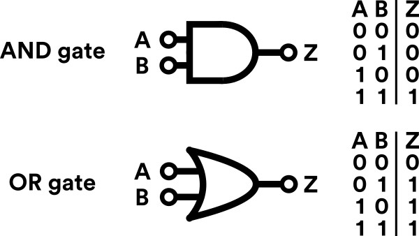
Perhaps the two most intuitive examples of this are the AND and OR gates. With an AND gate the output of its function is 1 when both the inputs are 1 (or in other words, when A AND B are 1). With an OR gate the output of its function is 1 when either of the inputs are 1 (or in other words, when A OR B is 1).
Figure 1 shows a simple diagram of both the AND and OR logic gates, along with their associated truth tables - which show what the output of the gate is for each possible input:
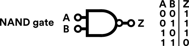
Of course, AND and OR are just two examples of fundamental logic gates. But a curious logic gate to explore further is the NAND gate (NOT AND) - because it has a rather special property: 'functional completeness'.
The 'universal' NAND gate
The NAND (NOT AND) gate is special because any boolean function can be implemented by using a combination of NAND gates (that's the 'functional completeness' bit). Or, in other words, you can use a combination of NAND gates to represent any other logic gate.
It is similar to an AND gate, except that its output is inverted (that's the NOT part!). Figure 2 shows the symbol and truth table of the gate.
As the NAND gate can be used to represent any other logic gate it can be thorght of as a 'universal' logic gate. You can build any digital logic based component from a NAND gate - if you are so inclined you could even build your own computer entirely out of them! In fact, some people have!
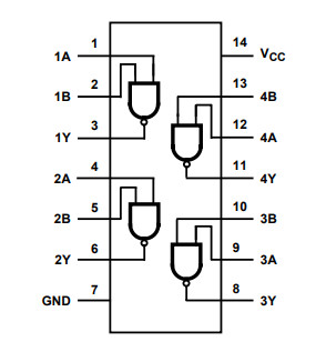
For the curious, NAND gates can be used or implemented in a practical sense using the classic 74HC00 integrated circuit. This chip is a quad two-input NAND gate and is based on CMOS technology. You can view the data sheet here.
But before you go off to build your own NAND gate computer, lets look at how NAND gates can be used to create a very important component in the world of computational hardware: the D-Type Flip-Flop.
Remembering things: the D-type Flip Flop
Logic gates are powerful components, but their purpose is not limited to trivial logic functions. Logic gates can also be used to perform 'sequential logic' - meaning that they can also be used to remember information (which is pretty neat).
To enable this, logic gates need to be arranged to create a 'latching' mechanism to store a particular piece of data. Often this mechanism is a 'clock' signal, which can be edge-triggered or level-triggered (edge-triggered events occur when the clock signal transitions from low-to-high, level-triggered events occur when the clock signal is high).
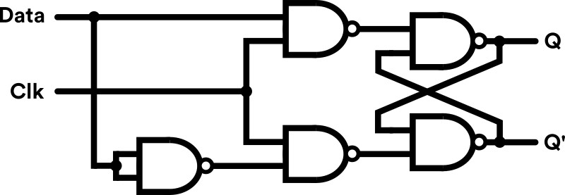
A good example of this particular mechanisms, or circuit, is the D-type flip-flop (yes, odd name) - pictured in figure 4.
This circuit comprises of five NAND gates (yep, everybody's favourite new gate), with two inputs and two outputs: a data input (Data), a clock signal (Clk), the latched data (Q) and its inverse (Q'), respectively. Those already familiar with sequential logic will also spot the SR flip-flop arrangement to the rightmost of the figure.
The D-type flip-flop operates in a very simply manner: When Clk is high (1) the output, Q, is set to the value of Data (0 or 1) at that moment in time. When Clk is low (0) Q retains its value/state regardless of what the Data value is. Q' is always the inverse of Q.
Of course, this may seem like a slightly trivial example, but lets look at the 74HC173 - an integrated circuit which houses multiple D-type flips-flops togeather in a single package.
A 4-bit Register from D-type Flip-Flops
The 74HC173 is a quad D-type flip-flip IC. However, this IC doesn't just contain four isolated D-type flip-flops - it employs a common clock between them, enabling 4-bits of information to be synchronously stored in a single clock pulse! And this, in effect, enables to you to use the IC as a 4-bit register.

The 74HC173 contains a more complex array of D-type flip-flops than the basic configuration explored in figure 4, as the circuits include some additional features:
- A common clocking mechanism (CP pin) - operating as positive edge-triggered.
- Data enable pins (E1 & E2) - this enables the flip-flops to 'ignore' the clock signal which is useful in more complex digital circuit designs.
- Three-state mode outputs (OE1 & OE2) - this is useful when connecting the output pins in a bus configuration.
- A 'master reset' pin (MR) - which resets all Q output values to 0.
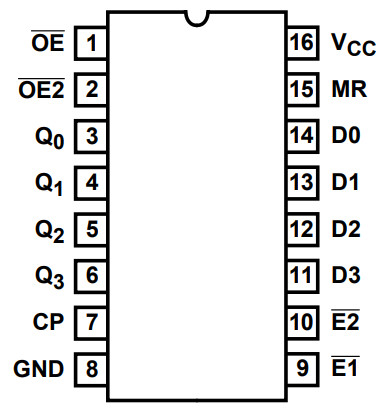
To understand this at a practical level, figure 6 shows the pinout of the 74HC173, where Dx are the data pins and Qx are the output pins. The common pins (CP, E1 & E2, OE1 & OE2 and MR) are also shown.
The 74HC173 is a great chip to explore and is used in a wide range of applications. Its operation and features make it ideal for use as a 4-bit register. Further exploration can be made through the 74HC173 datasheet. Or, to get hands on, why not check out our stock of 74HC173s and spare parts for IC exploration.
For the curious, our next note: ROM & RAM: An Introduction to Computer Memory explores how the concept of registers can be used to create computer memory.