A core part of a computer is the ability to store and fetch information. This note outlines the basics of computer memory, with an introduction to the two main memory types: ROM and RAM.
An Introduction to Computer Memory
Charles Babbage, the famous 19th century English mathematician and polymath, once said that for a machine to perform the functions of a human computer it must possess three things: a unit capable of performing the operations of arithmetic, a built-in power of judgement and a store.
The latter - a store - would retain the numbers and instructions required to define the successive stages in computation. Of course, in the 21st century we'd recognise this as 'computer memory', but in the 19th century this really was a groundbreaking idea.
But how does one go about mechanising memory? How does a thing remember other things? How did Babbage's ideas turn into reality?
To answer these questions lets first define, in modern terms, what we mean by a store, or the memory of a computational machine:
"The memory of a computer is where the program and data are stored before the calculations begin. During a computer run, the control section may store partial answers in the memory, similar to the way we use paper to record our work. The memory is therefore one of the most active parts of a computer, storing not only the program and data but processed data as well. The memory is equivalent to thousands of registers, each storing a binary word."
Perhaps the most important part of this excerpt is the idea that "memory is equivalent to thousands of registers". In our previous note: From Logic Gates to Registers: Exploring the 74HC173 we explored how registers - a fundamental digital electronics circuit - can be made from basic logic gates to remember, or store, a binary value. A computer's memory, as we know it today, can contain a vast array of registers or 'memory cells', which can be individually referenced (addressed) to recall the value stored within them.

Figure 1 shows a simple memory structure. Each register, or memory cell, can store a value of 4-bits (values stored in memory are often referred to as 'words' - in this case a 4-bit word), and can be addressed by a unique 3-bit binary value.
Of course, this is a simplified and generalised representation of how memory is structured, and to understand some of the complexities and differences in memory structures we must first understand the two major memory types: 'Random Access Memory' and 'Read Only Memory'.
Read Only Memory (ROM)
Read Only Memory is the simpler of the two major memory types. As per its name, it is a type of memory which is readable only. In other words - you cannot continually write new data to the memory - the information it contains is fixed before operation. This type of memory is also referred to as 'non-volatile', as it retains its data after it is powered off.
As ROMs are used for the permanent storage of data, it doesn't require a mechanism for continually writing data to the memory array. Therefore, in its most basic form, it can be constructed as a simple diode matrix - a popular technique for creating ROMs in the 1960s and 70s. Figure 2 shows the construction of a ROM diode matrix using the data values presented in figure 1.
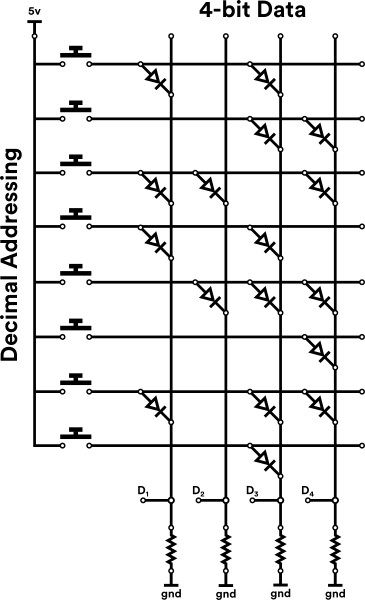
Figure 2 shows the layout of intersecting diodes, which are used in combination with a pull-down resistor configuration to 'encode' the data permanently. The data can be addressed (in this example using a decimal addressing system) by enabling one of the push switches to select the active line of diodes (you can think of each line or row of diodes as a read-only register). Once an active line is selected the 4-bit data encoded by the diodes will appear as a binary output at the data lines D1-D4.
Diode matrices are rarely used in modern times as they are difficult to scale up due to the physical constraints of the hardware. Instead they have been replaced with semiconductor ICs which can store a vast amount of data in a very small footprint.
Since the 60s and 70s, a few different types of semiconductor ROM technologies have evolved enabling an engineer to program them, these technologies include: PROM, EPROM, and EEPROM!
A PROM (Programmable ROM) uses an instrument called a PROM programmer to 'burn' the pattern of bits (data) onto the chip through an array of fusible links. The limitation to this technology is that it is a 'one time' process - data cannot be reprogrammed later on. The EPROM (Erasable Programmable ROM) overcomes this problem by enabling the data to be stored on a chip electronically and it can be erased and reprogrammed by exposing the chip to UV radiation.
Finally, EEPROM (Electrically Erasable Programmable ROM) enables data to be programmed and erased in-circuit by applying special signals to the ICs during the programming process. However, the amount of times the chip can be programmed is limited.
Figure 3 shows a picture of a common EEPROM IC, the AT28C256-15PU: a high performance 256K (32K x 8bit) EEPROM in a 28 pin DIP package.

In the next section we will explore the other major memory type - RAM, and the differences in being writable and volatile.
Random Access Memory (RAM)
Random Access Memory is a type of memory which is both readable and writeable, it is referred to as 'random access' as all the stored data words can be read equally quickly.
Unlike ROM, RAM is a type of volatile memory. This means that the data stored in its memory is lost when the power to it is switched off.
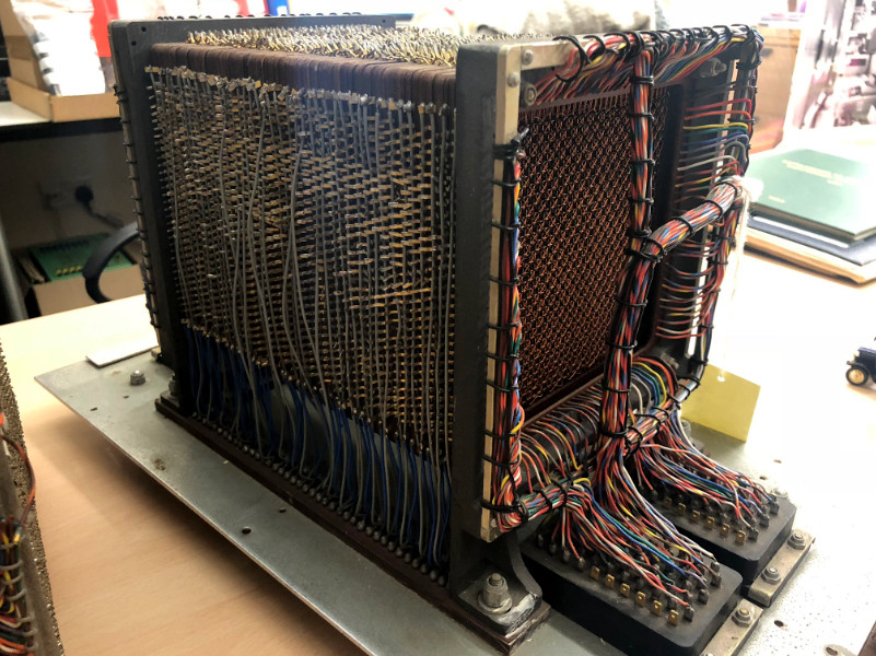
The technological developments driving RAM technology have changed significantly since the early days of computing. In the late 1940s through to the 1970s magnetic-core memory was a standard technology for implementing RAM. However, this archaically beautiful technology this was later replaced by semiconductor ICs in the 1970s.
The two most widely used forms of modern semiconductor RAM are dynamic (DRAM) and static (SRAM). Dynamic RAM uses a transistor and capacitor pair for each memory bit - however the capacitor must be refreshed constantly increasing the power consumption of the device. Static RAM uses a flip-flop configuration for each memory bit, which uses less power than DRAM, but is more expensive and has a lower storage density.
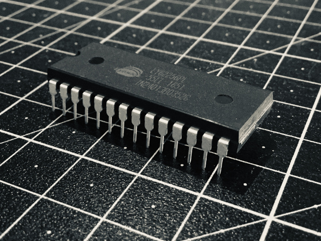
Figure 6 shows a 32k 8-bit through-hole SRAM IC - a popular IC in computational hardware projects (and significantly smaller than the magnetic-core memory of the 1940s!).
Returning to the anatomy of memory, RAM ICs are fairly simple devices and can be considered as "marshalls" to an array of writeable memory cells. Figure 7 shows the layout of a very basic RAM device, in this case an 8 x 4-bit example:
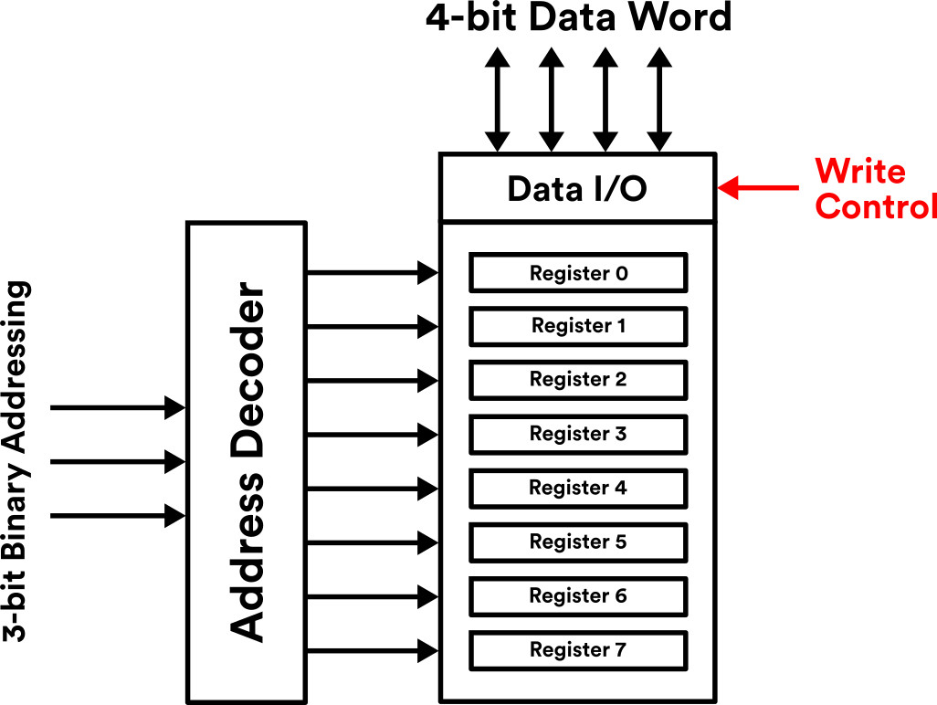
In the above diagram, the 'address decoder' converts a 3-bit binary value into 8 locations and the 'data word' can be input and output from the device through the 'Data I/O' interface. The latter is usually controlled through special control pins on an IC, in this case denoted by the 'Write Control'.
(It is also worth remembering that addresses are referenced using binary values, therefore they exist in increasing powers of two. Hence why address space is often referred to with seemingly strange values: 32k 64k 128k etc).
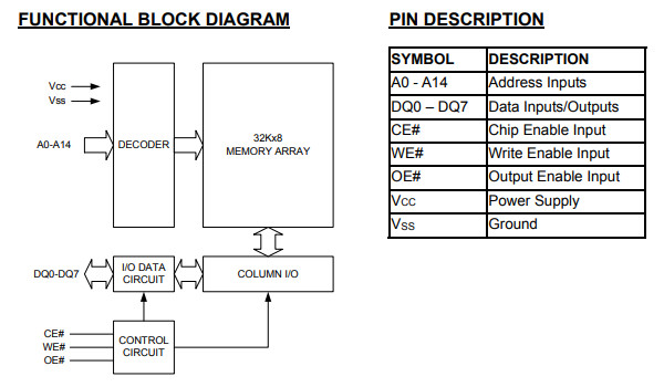
Following on from figure 6 & 7, and as a real-life example, lets now take a closer look at the 32k 8-bit LY62256PL's functional block diagram and pin description (taken from the datasheet). This is easily comparable with the basic anatomy in figure 7 but differs in the number of pins required to give a greater address range and data word size:
And believe it or not, that really is RAM in a nutshell - not as complex as one might think!
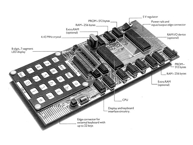
Babbage's Store in Action
In this note we've explored the two fundamental forms of memory in a computer system: ROM & RAM. These technologies are used in modern machines to store software, firmware and microcode - enabling information to be processed using the mechanisms of computation.
We've seen how both analogue and digital electronics can be used to store and remember information, we've explored the anatomy of how memory works in an abstract sense, and seen common ROM & RAM ICs that you can buy from a supplier for a few pounds!
It really is quite remarkable to think that 'the store' that Charles Babbage humbly imagined hundreds of years ago has evolved into a marvel of modern engineering. I do wonder what he would say if he were alive today...